Capabilities
Alert
We do not recommend this page on mobile phone
Know Metanoia’s Capabilities & Get your PCBs Built Fast
Note
There is no Plated Through Hole in the two layers
 Through Hole Plating (الترسيب)
https://www.youtube.com/watch?v=badMYPchBqg
 Through Hole Plating (الترسيب)
https://www.youtube.com/watch?v=badMYPchBqg
PCB
3D printing
PCB
PCB Specifications
| Features | capability | Note | Example |
|---|---|---|---|
| Layer count | 1,2 Layers | The number of copper layers in the board. | |
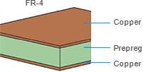
| Material | FR-4 | FR-4 Standard Tg 130-140/ Tg 155 |
|
| Max. Dimension | 170x290mm | The maximum dimension Metanoia can accept |

|
Drill Size
| Features | capability | Note | Example |
|---|---|---|---|
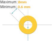
| Drill Hole Size | 0.60mm- 8mm | Min. drill size is 0.20mm. Max. drill size is 8mm. |
|
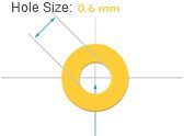
| Min. Via hole size | 0.6mm | For Single&Double Layer PCB, the minimum via hole size is 0.6mm |
|
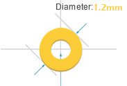
| Min. Via diameter | 1.2mm | For Single&Double Layer PCB, the minimum Via diameter is 1.2mm |
|
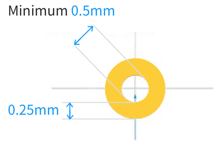
| Pad Size | Minimum 1.2mm | The pad size will be enlarged by 0.5mm than the hole size. The minimum size of annular ring around plated through hole pads is 0.3mm. If the recommended sizes are not respected then the pad will not be produced properly. |
|
| Min. Non-Plated Slots | 1.0mm | The minimum Non-Plated Slot Width is 1.0mm, please draw the slot outline in the mechanical layer(GML or GKO) |
|
Minimum clearance
| Features | capability | Example |
|---|---|---|
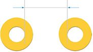
| Hole to hole clearance(Different nets) | 0.6mm |
|
| Via to Via clearance(Same nets) | 0.4mm |

|
| Pad to Pad clearance(Pad without hole, Different nets) | 0.4mm |

|
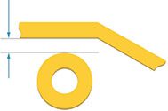
| Via to Track | 0.3mm |

|
| Pad to Track | 0.4mm |
|
Minimum trace width and spacing
| Min . Trace Width | Min . Trace Spacing | Example | |
|---|---|---|---|
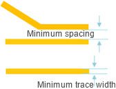
| 1-2 Layers | 0.4mm | 0.4mm |
|
3D printing