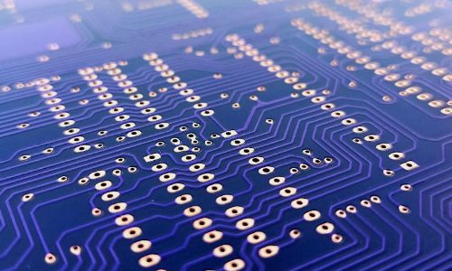
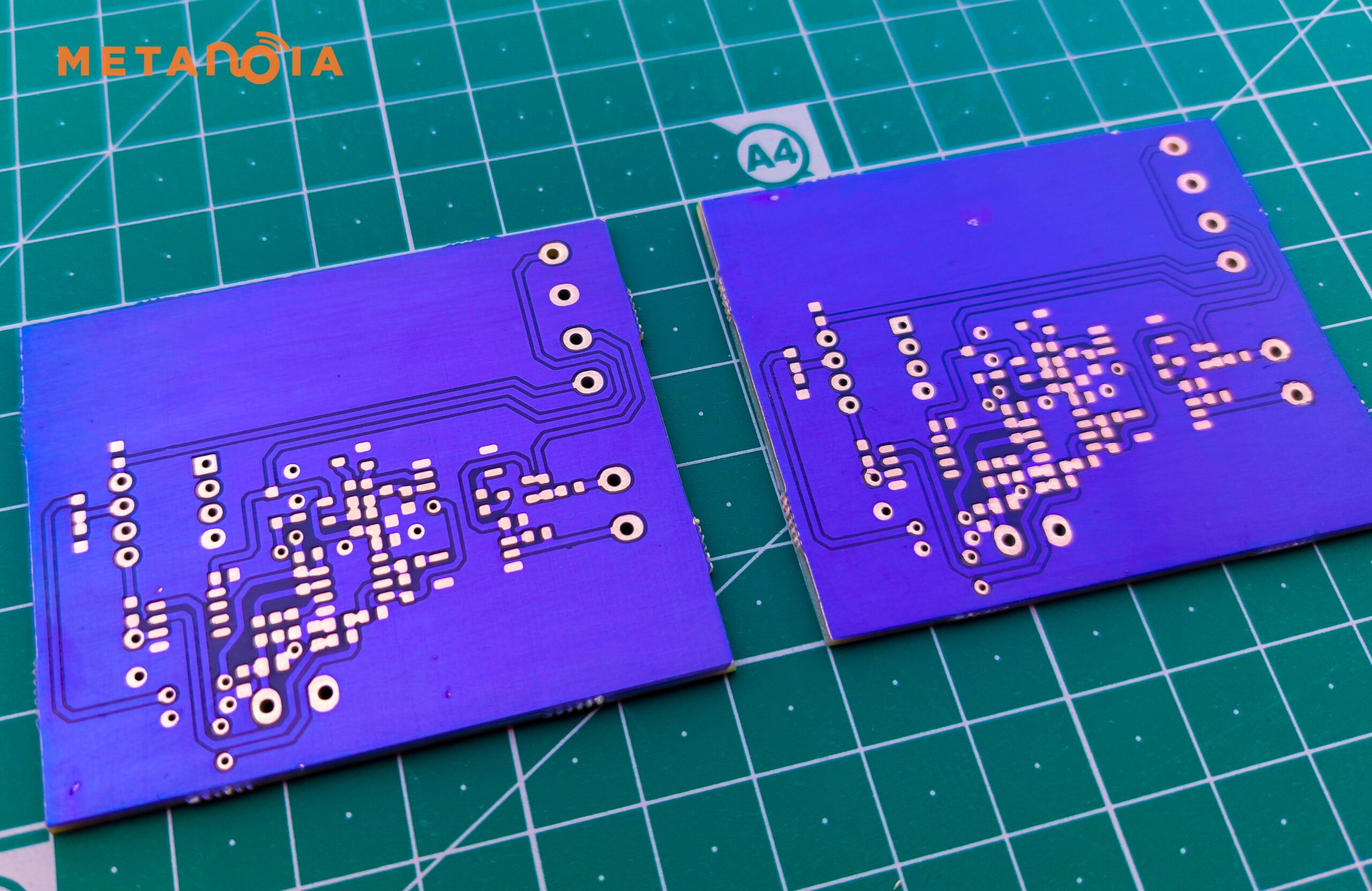
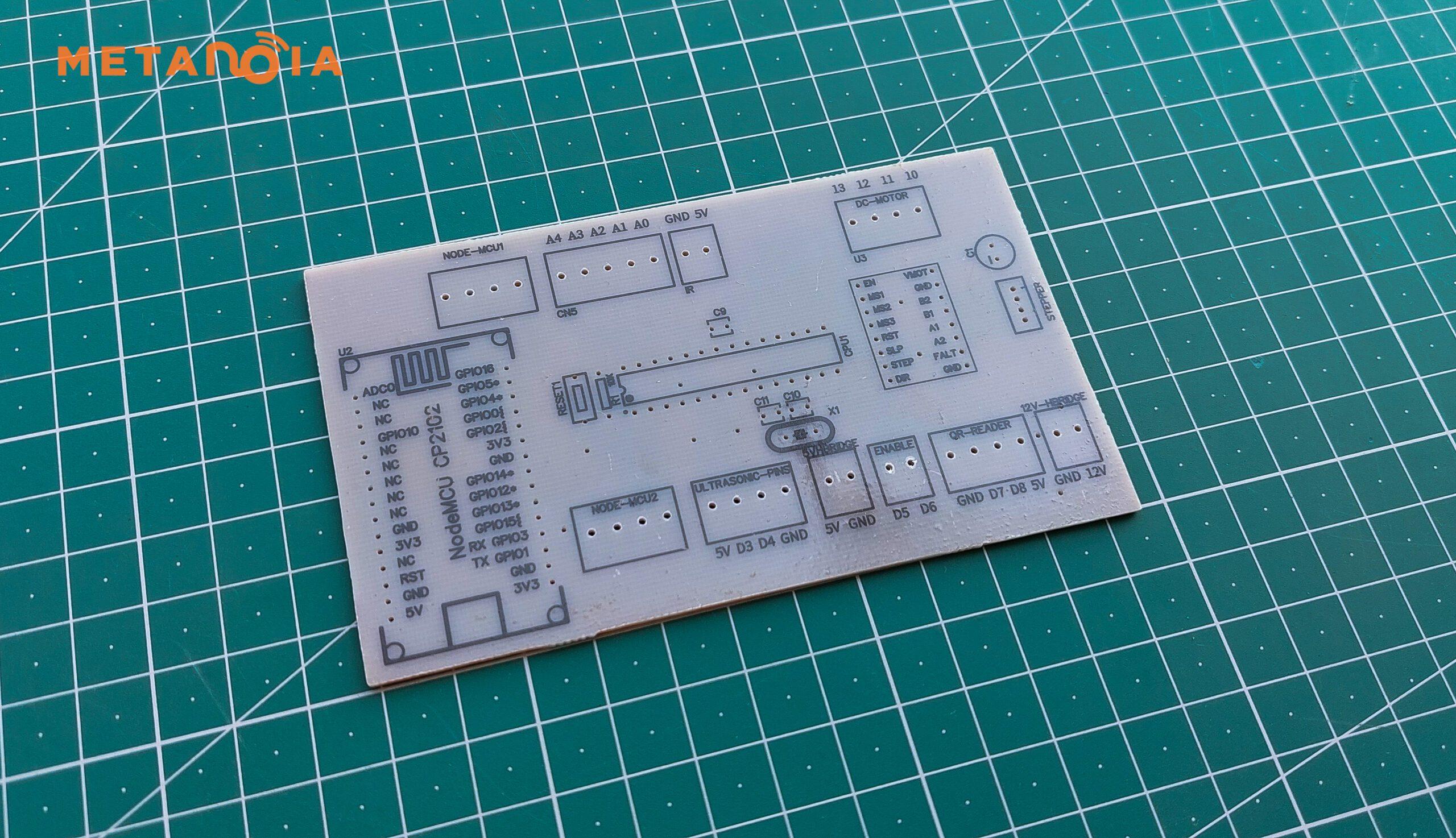
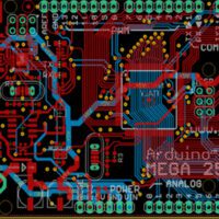
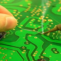
PCB or Printed Circuit Board is the traditional name for the bare board on which you supply us with the layout data and which you use to mount your components once we have delivered it to you.
A printed circuit board, or PCB, is used to mechanically support and electrically connect electronic components using conductive pathways, tracks or signal traces etched from copper sheets laminated onto a non-conductive substrate.
When the board has only copper tracks and features, and no circuit elements such as capacitors, resistors, or active devices have been manufactured into the actual substrate of the board, it is more correctly referred to as a printed wiring board (PWB) or etched wiring board.
Use of the term PWB or printed wiring board although more accurate and distinct from what would be known as a true printed circuit board has generally fallen by the wayside for many people as the distinction between circuit and wiring has become blurred.
Today printed wiring (circuit) boards are used in virtually all but the simplest commercially produced electronic devices and allow fully automated assembly processes that were not possible or practical in earlier era tag-type circuit assembly processes.
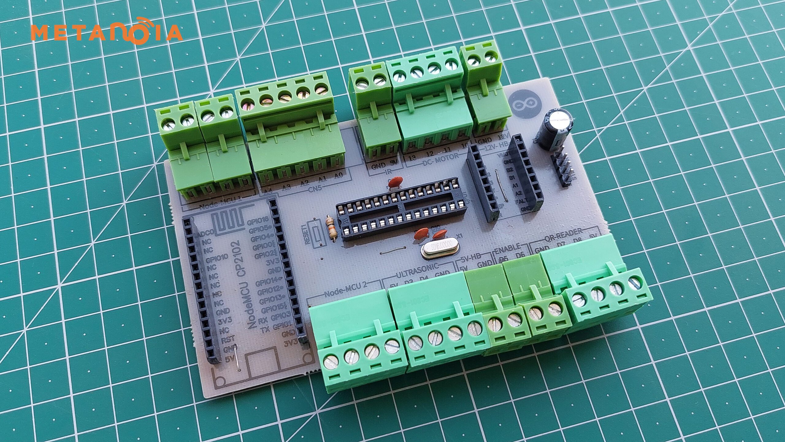
A PCB populated with electronic components is called a printed circuit assembly (PCA), printed circuit board assembly, or PCB Assembly (PCBA). In informal use the term “PCB” is used both for bare and assembled boards, the context clarifying the meaning.
